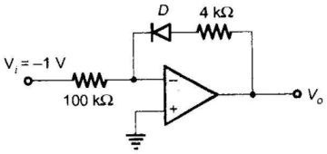
Consider the following circuit using an ideal op-amp. The I-V characteristics of the diode is described by the relation $${\text{I}} = {{\text{I}}_0}\left( {{{\text{e}}^{\frac{{\text{V}}}{{{{\text{V}}_{\text{T}}}}}}} - 1} \right)$$ where VT = 25 mV, I0 = 1 µA and V is the voltage across the diode (taken as positive for forward bias).
For an input voltage Vi = -1 V, the output voltage V0 is

A. 0 V
B. 0.1 V
C. 0.7 V
D. 1.1 V
Answer: Option B
Related Questions on Analog Electronics
The action of JFET in its equivalent circuit can best be represented as a
A. Current controlled Current source
B. Current controlled voltage source
C. Voltage controlled voltage source
D. Voltage controlled current source
In a p+n junction diode under reverse bias, the magnitude of electric field is maximum at
A. The edge of the depletion region on the p-side
B. The edge of the depletion region on the n-side
C. The p+n junction
D. The center of the depletion region on the n-side
To prevent a DC return between source and load, it is necessary to use
A. Resistor between source and load
B. Inductor between source and load
C. Capacitor between source and load
D. Either A or B

Join The Discussion