11. As compared to a full wave rectifier using 2 diodes, the four diode bridge rectifier has the dominant advantage of
12. For a full-wave rectifier with shunt capacitor filter, the peak to peak ripple voltage is
(where f = fundamental power line frequency, IDC = DC current)
(where f = fundamental power line frequency, IDC = DC current)
13. In a multi-stage RC-coupled amplifier the coupling capacitor.
14. An amplifier has a D.C. power supply of 15 V and draws a current of 10 mA. It produces an output of 5 V peak across a load resistance of 600 Ω for a signal frequency of 1 kHz. What will be its A.C. power output?
15. Determine the change in collector current, ∆IC due to change in base emitter voltage VBE from 25°C to 100°C for a Silicon Transistor in Fixed Bias Configuration having β = 100.
(Consider following variation in Silicon transistor parameters with temperature-At T = 25°C, VBE = 0.65 V and At T = 100°C. VBE = 0.5 V)
(Consider following variation in Silicon transistor parameters with temperature-At T = 25°C, VBE = 0.65 V and At T = 100°C. VBE = 0.5 V)
16. While using a bipolar junction transistor as an amplifier, the collector and emitter terminals got interchanged mistakenly. Assuming that the amplifier is a common emitter amplifier and the biasing is suitably adjusted, the interchange of terminals will results into which one of the following?
17. BJT is three terminal device which stands for bipolar junction transistor. Which of the following are true about BJT.
1. Base has smallest area to reduce the transit time.
2. collector is provided with the largest area to withstand heat dissipation.
3. BJT is a current controlled device.
4. BJT is a voltage controlled device.
1. Base has smallest area to reduce the transit time.
2. collector is provided with the largest area to withstand heat dissipation.
3. BJT is a current controlled device.
4. BJT is a voltage controlled device.
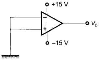
18. If the op-amp in the figure has an input offset voltage of 5 mV and an open-loop voltage gain of 10,000, then V0 will be

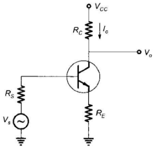
19. The feedback topology in the amplifier circuit (the base bias circuit is not shown for simplicity) in the figure is

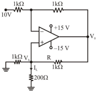
20. What is the load current IL in the circuit below?

Read More Section(Analog Electronics)
Each Section contains maximum 100 MCQs question on Analog Electronics. To get more questions visit other sections.
