41. The dissipation at the collector is zero in the quiescent state and increase with excitation in the case of a
42. The responsivity of the PIN photodiode shown is 0.9 A/W. To obtain Vout of -1 V for an incident optical power of 1 mW, the value of R to be used is
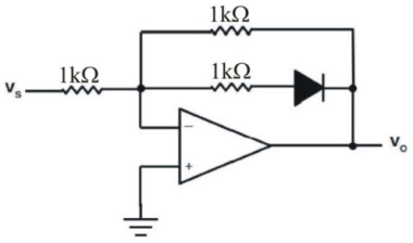
43. In the circuit shown below assume that diodes and op-amp are ideal. Suppose that V01 is the output voltage when input voltage is Vs = -1.0 V and V02 is the output voltage when input voltage is Vs = +1.0 V, then the value of V01 + V02 is

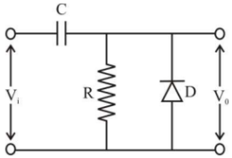
44. The circuit shown in figure is a

45. Consider the following circuit using an ideal op-amp. The I-V characteristics of the diode is described by the relation $${\text{I}} = {{\text{I}}_0}\left( {{{\text{e}}^{\frac{{\text{V}}}{{{{\text{V}}_{\text{T}}}}}}} - 1} \right)$$ where VT = 25 mV, I0 = 1 µA and V is the voltage across the diode (taken as positive for forward bias).
For an input voltage Vi = -1 V, the output voltage V0 is
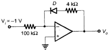
For an input voltage Vi = -1 V, the output voltage V0 is

46. A second-order band-pass active filter can be obtained by cascading a low-pass second-order section having cut-off frequency fOH with a high-pass second-order section having cut-off frequency fOL, provided
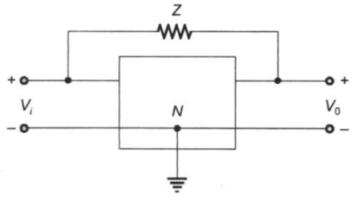
47. In the circuit shown in figure is a finite gain amplifier with a gain of K, a very large input impedance, and a very low output impedance. The input impedance of the feedback amplifier with the feedback impedance Z connected as shown will be

48. In a log amplifier the input is 'a'. The output will be proportional to
49. Diodes are used to clip voltages in circuits because they act as:
50. An n-type MOSFET and an npn BJT are biased so that IC = ID = 1 mA, VGS = 1.3 V and VBE = 0.7 V. Threshold voltage for the MOSFET is 0.8 V and thermal voltage at the ambient temperature is given to be 25 mV. Transconductances of the BJT and the MOSFET are:
Read More Section(Analog Electronics)
Each Section contains maximum 100 MCQs question on Analog Electronics. To get more questions visit other sections.
