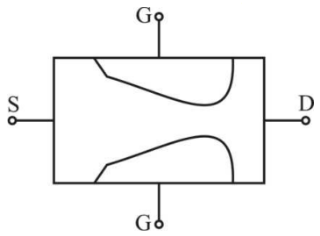
51. What is one of the primary advantages of FET compared to BJT?
52. Why is silicon dioxide (SiO2) layer used in ICs?
53. In a biased JFET, the shape of the channel is as shown in the given figure. because


54. Practically, in order to create an electron-hole pair in a P-N junction diode, the energy of the incident photon should be
55. In order to generate electron-hole pairs, the maximum wavelength of radiation for Silicon (Band gap = 1.1 eV) is
56. The diffusion potential across P-N junction
57. The quantum efficiency η for the photo detector is
Where,
Iph = Average photocurrent
Pe = Average incident optical power
hc/λ = Incident photon energy
Where,
Iph = Average photocurrent
Pe = Average incident optical power
hc/λ = Incident photon energy
58. Which statement is correct for Schottky diode?
59. Assuming that the electron mobility in intrinsic silicon is 1500 cm2/V-Sec at room temperature (T = 300 K and the corresponding 'volt equivalent of temperature' VT = 25.9 mV, what is the approximate value of the electron diffusion constant?
60. In a forward-biased p-n diode with NA >> ND, the product of dynamic diode resistance and diffusion capacitance CD equals:
Read More Section(Electronic Devices and Circuits)
Each Section contains maximum 100 MCQs question on Electronic Devices and Circuits. To get more questions visit other sections.
