31.
A ripple counter designed with J-K flip-flops provided with CLEAR (Cl.) input is shown in the figure. In order that this circuit functions as a MOD-12 counter, the NAND gate inputs (X1 and X2) should be
Electronics mcq question image

32.
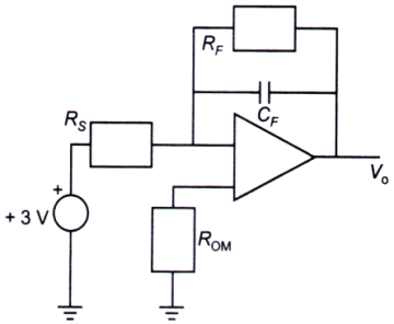
Figure shows a practical integrator with Rs = 30 M$$\Omega $$, RF = 20 M$$\Omega $$ and CF = 0.1 μF. If a step (DC) voltage of +3 V is applied as input for 0 ≤ t ≤ 4 (t is in second), the output voltage is
Electronics mcq question image

33.
Under normal operating conditions, the gate terminals of an n-channel Junction Field Effect Transistor UFET) and an n-channel Metal Oxide Semiconductor Field Effect Transistor (MOSFET) are

34.
The registers QD, QC, QB and QA shown in the figure are initially in the state 1010 respectively. An input sequence SI = 0101 is applied. After two clock pulses, the state of the shift registers (in the same sequence QD QC QB QA) is
Electronics mcq question image

36.
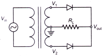
For the rectifier circuit shown in the figure, the sinusoidal voltage (V1 or V2) at the output of the transformer has a maximum value of 10 V. The load resistance RL, is 1 k$$\Omega $$. If lav is the average current through the resistor RL, the circuit corresponds to a
Electronics mcq question image

37.
Which one of the following is true for a semiconductor p-n junction with no external bias?