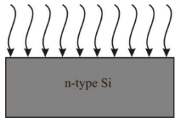
Consider a silicon sample at T = 300 K, with a uniform donor density Nd = 5 × 1016 cm-3 illuminated uniformly such that the optical generation rate is Gopt = 1.5 × 1020 cm-3 s-1 throughout the sample. The incident radiation is turned off at t = 0. Assume low-level injection to be valid and ignore surface effects. The carrier lifetimes are τp0 = 0.1 µs and τn0 = 0.5 µs.
The hole concentration at t = 0 and the hole concentration at t = 0.3 µs, respectively, are

A. 1.5 × 1013 cm-3 and 7.47 × 1011 cm-3
B. 1.5 × 1013 cm-3 and 8.23 × 1011 cm-3
C. 7.5 × 1013 cm-3 and 3.73 × 1011 cm-3
D. 7.5 × 1013 cm-3 and 4.12 × 1011 cm-3
Answer: Option A
The forbidden energy gap between the valence band and conduction band will be least in case of
A. Metals
B. Semiconductors
C. Insulators
D. All of the above
For a NPN bipolar transistor, what is the main stream of current in the base region?
A. Drift of holes
B. Diffusion of holes
C. Drift of electrons
D. Diffusion of electrons
A. Both A and R are true and R is correct explanation of A
B. Both A and R are true but R is not a correct explanation of A
C. A is true but R is false
D. A is false but R is true
For a P-N diode, the number of minority carriers crossing the junction depends on
A. Forward bias voltage
B. Potential barrier
C. Rate of thermal generation of electron hole pairs
D. None of the above

Join The Discussion