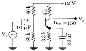
An amplifier circuit is shown in the given figure:
The voltage gain $$\left( {\frac{{{{\text{V}}_0}}}{{{{\text{V}}_{\text{s}}}}}} \right)$$ is:

A. $$\frac{4}{{3.33}}$$
B. 100
C. 150
D. 160
Answer: Option D
Related Questions on Analog Electronics
The action of JFET in its equivalent circuit can best be represented as a
A. Current controlled Current source
B. Current controlled voltage source
C. Voltage controlled voltage source
D. Voltage controlled current source
In a p+n junction diode under reverse bias, the magnitude of electric field is maximum at
A. The edge of the depletion region on the p-side
B. The edge of the depletion region on the n-side
C. The p+n junction
D. The center of the depletion region on the n-side
To prevent a DC return between source and load, it is necessary to use
A. Resistor between source and load
B. Inductor between source and load
C. Capacitor between source and load
D. Either A or B

Join The Discussion