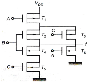
In figure T1, T2 and T3 are p-channel MOS transistors, and T4, T5 and T6 are n-channel MOS transistors. A, B and C are binary signals. The output f(A, B, C) is

A. $$\overline {\text{A}} \left( {\overline {\text{B}} + \overline {\text{C}} } \right)$$
B. A + BC
C. A(B + C)
D. ABC
Answer: Option A
The action of JFET in its equivalent circuit can best be represented as a
A. Current controlled Current source
B. Current controlled voltage source
C. Voltage controlled voltage source
D. Voltage controlled current source
In a p+n junction diode under reverse bias, the magnitude of electric field is maximum at
A. The edge of the depletion region on the p-side
B. The edge of the depletion region on the n-side
C. The p+n junction
D. The center of the depletion region on the n-side
To prevent a DC return between source and load, it is necessary to use
A. Resistor between source and load
B. Inductor between source and load
C. Capacitor between source and load
D. Either A or B

Join The Discussion