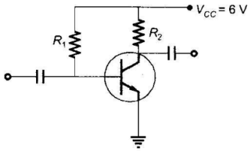
In the amplifier circuit shown in the figure, the values of R1 and R2 are such that the transistor is operating at VCE = 3 V and IC = 1.5 mA when its β is 150. For a transistor with β of 200, the operating point (VCE, IC) is

A. (2 V, 2 mA)
B. (3 V, 2 mA)
C. (4 V, 2 mA)
D. (4 V, 1 mA)
Answer: Option A
Related Questions on Analog Electronics
The action of JFET in its equivalent circuit can best be represented as a
A. Current controlled Current source
B. Current controlled voltage source
C. Voltage controlled voltage source
D. Voltage controlled current source
In a p+n junction diode under reverse bias, the magnitude of electric field is maximum at
A. The edge of the depletion region on the p-side
B. The edge of the depletion region on the n-side
C. The p+n junction
D. The center of the depletion region on the n-side
To prevent a DC return between source and load, it is necessary to use
A. Resistor between source and load
B. Inductor between source and load
C. Capacitor between source and load
D. Either A or B

Join The Discussion