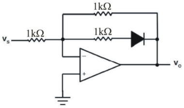
In the circuit shown below assume that diodes and op-amp are ideal. Suppose that V01 is the output voltage when input voltage is Vs = -1.0 V and V02 is the output voltage when input voltage is Vs = +1.0 V, then the value of V01 + V02 is

A. 2.0 V
B. -0.5 V
C. 0.5 V
D. 0.0 V
Answer: Option C
Related Questions on Analog Electronics
The action of JFET in its equivalent circuit can best be represented as a
A. Current controlled Current source
B. Current controlled voltage source
C. Voltage controlled voltage source
D. Voltage controlled current source
In a p+n junction diode under reverse bias, the magnitude of electric field is maximum at
A. The edge of the depletion region on the p-side
B. The edge of the depletion region on the n-side
C. The p+n junction
D. The center of the depletion region on the n-side
To prevent a DC return between source and load, it is necessary to use
A. Resistor between source and load
B. Inductor between source and load
C. Capacitor between source and load
D. Either A or B

Join The Discussion