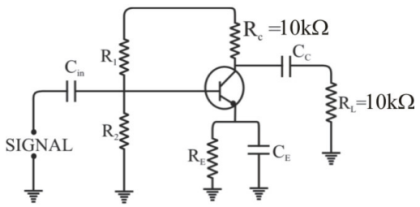
In the circuit shown below, if RC = 10 kΩ, RL = 10 kΩ, β = 100, input signal voltage is 1 mV r.m.s. The output voltage is:

A. 100 V
B. 150 V
C. 250 V
D. 350 V
E. 200 V
Answer: Option E

A. 100 V
B. 150 V
C. 250 V
D. 350 V
E. 200 V
Answer: Option E
The action of JFET in its equivalent circuit can best be represented as a
A. Current controlled Current source
B. Current controlled voltage source
C. Voltage controlled voltage source
D. Voltage controlled current source
In a p+n junction diode under reverse bias, the magnitude of electric field is maximum at
A. The edge of the depletion region on the p-side
B. The edge of the depletion region on the n-side
C. The p+n junction
D. The center of the depletion region on the n-side
To prevent a DC return between source and load, it is necessary to use
A. Resistor between source and load
B. Inductor between source and load
C. Capacitor between source and load
D. Either A or B
Join The Discussion