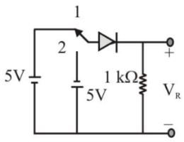
In the circuit shown below, the switch was connected to position 1 at t < 0 and at t = 0, it is changed to position 2. Assume that the diode has zero voltage drop and a storage time ts. For 0 < t ≤ ts.VRs given by (all in Volts)

A. VR = -5
B. VR = +5
C. 0 ≤ VR < 5
D. -5 < VR < 0
Answer: Option A
Related Questions on Analog Electronics
The action of JFET in its equivalent circuit can best be represented as a
A. Current controlled Current source
B. Current controlled voltage source
C. Voltage controlled voltage source
D. Voltage controlled current source
In a p+n junction diode under reverse bias, the magnitude of electric field is maximum at
A. The edge of the depletion region on the p-side
B. The edge of the depletion region on the n-side
C. The p+n junction
D. The center of the depletion region on the n-side
To prevent a DC return between source and load, it is necessary to use
A. Resistor between source and load
B. Inductor between source and load
C. Capacitor between source and load
D. Either A or B

Join The Discussion