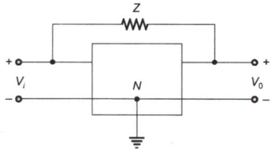
In the circuit shown in figure is a finite gain amplifier with a gain of K, a very large input impedance, and a very low output impedance. The input impedance of the feedback amplifier with the feedback impedance Z connected as shown will be

A. $${\text{Z}}\left[ {1 - \frac{1}{{\text{K}}}} \right]$$
B. $${\text{Z}}\left( {1 - {\text{K}}} \right)$$
C. $$\left[ {\frac{{\text{Z}}}{{{\text{K}} - 1}}} \right]$$
D. $$\left[ {\frac{{\text{Z}}}{{1 - {\text{K}}}}} \right]$$
Answer: Option D
The action of JFET in its equivalent circuit can best be represented as a
A. Current controlled Current source
B. Current controlled voltage source
C. Voltage controlled voltage source
D. Voltage controlled current source
In a p+n junction diode under reverse bias, the magnitude of electric field is maximum at
A. The edge of the depletion region on the p-side
B. The edge of the depletion region on the n-side
C. The p+n junction
D. The center of the depletion region on the n-side
To prevent a DC return between source and load, it is necessary to use
A. Resistor between source and load
B. Inductor between source and load
C. Capacitor between source and load
D. Either A or B

Join The Discussion