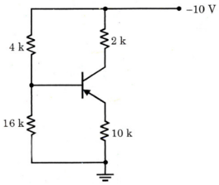
In the circuit shown in the given figure, the approximate voltage at the transistor

A. base and emitter respectively are -8 V and -7.3 V
B. base and collector respectively are -8 V and -5 V
C. collector and emitter respectively are -8 V and -7.3 V
D. base, emitter and collector respectively are -8 V, -7.3 and -5 V
Answer: Option A
The action of JFET in its equivalent circuit can best be represented as a
A. Current controlled Current source
B. Current controlled voltage source
C. Voltage controlled voltage source
D. Voltage controlled current source
In a p+n junction diode under reverse bias, the magnitude of electric field is maximum at
A. The edge of the depletion region on the p-side
B. The edge of the depletion region on the n-side
C. The p+n junction
D. The center of the depletion region on the n-side
To prevent a DC return between source and load, it is necessary to use
A. Resistor between source and load
B. Inductor between source and load
C. Capacitor between source and load
D. Either A or B

Join The Discussion