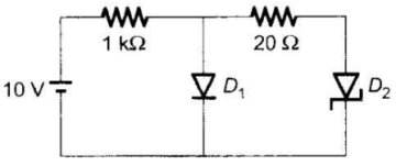
In the figure, assume that the forward voltage drops of the PN diode D1 and Schottky diode D2 are 0.7 V and 0.3 V, respectively. If ON denotes conducting state of the diode and OFF denotes non-conducting state of the diode, then in the circuit,

A. Both D1 and D2 are ON
B. D1 is ON and D2 is OFF
C. Both D1 and D2 are OFF
D. D1 is OFF and D2 is ON
Answer: Option D
The action of JFET in its equivalent circuit can best be represented as a
A. Current controlled Current source
B. Current controlled voltage source
C. Voltage controlled voltage source
D. Voltage controlled current source
In a p+n junction diode under reverse bias, the magnitude of electric field is maximum at
A. The edge of the depletion region on the p-side
B. The edge of the depletion region on the n-side
C. The p+n junction
D. The center of the depletion region on the n-side
To prevent a DC return between source and load, it is necessary to use
A. Resistor between source and load
B. Inductor between source and load
C. Capacitor between source and load
D. Either A or B

Join The Discussion