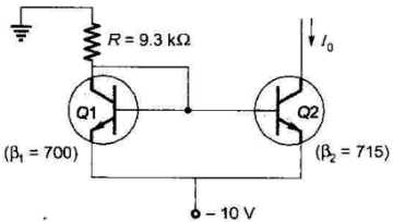
In the silicon BJT circuit shown below, assume that the emitter area of transistor Q1 is half that of transistor Q2.
The value of current I0 is approximately

A. 0.5 mA
B. 2 mA
C. 9.3 mA
D. 15 mA
Answer: Option B
Related Questions on Analog Electronics
The action of JFET in its equivalent circuit can best be represented as a
A. Current controlled Current source
B. Current controlled voltage source
C. Voltage controlled voltage source
D. Voltage controlled current source
In a p+n junction diode under reverse bias, the magnitude of electric field is maximum at
A. The edge of the depletion region on the p-side
B. The edge of the depletion region on the n-side
C. The p+n junction
D. The center of the depletion region on the n-side
To prevent a DC return between source and load, it is necessary to use
A. Resistor between source and load
B. Inductor between source and load
C. Capacitor between source and load
D. Either A or B

Join The Discussion