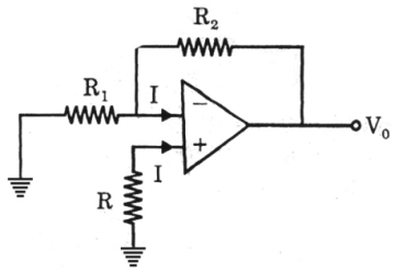
Which one of the following conditions would give Vo = 0 in the circuit shown in the figure?

A. R = R1 + R2
B. $${\text{R}} = \frac{{{{\text{R}}_2}}}{{{{\text{R}}_1}}}$$
C. R = R2 - R1
D. R = R1||R2
Answer: Option D
The action of JFET in its equivalent circuit can best be represented as a
A. Current controlled Current source
B. Current controlled voltage source
C. Voltage controlled voltage source
D. Voltage controlled current source
In a p+n junction diode under reverse bias, the magnitude of electric field is maximum at
A. The edge of the depletion region on the p-side
B. The edge of the depletion region on the n-side
C. The p+n junction
D. The center of the depletion region on the n-side
To prevent a DC return between source and load, it is necessary to use
A. Resistor between source and load
B. Inductor between source and load
C. Capacitor between source and load
D. Either A or B

Join The Discussion