21. The voltage divider bias circuit is used in amplifiers quit often because it
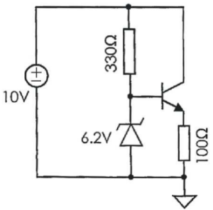
22. The zener diode shown in following figure is temperature compensated and current gain β of transistor is very high. If current through 100 ohm resistor is 55 mA at 25°C, what is the approximate current through it at 65°C

23. The output time period of a transistorized monostable multivibrator using base resistance Rb and coupling capacitor Cb for the output transistor is given by
24. In a BJT, the Ic = 30 mA. If β = 100, the base current approximately equals
25. Negative voltage feedback in amplifiers
S1: Improves gain stability
S2: Reduces non linear distortion
S3: Improves frequency response
S4: Increase circuit stability
S5: Increase Input Impedance and decrease output impedance
S1: Improves gain stability
S2: Reduces non linear distortion
S3: Improves frequency response
S4: Increase circuit stability
S5: Increase Input Impedance and decrease output impedance
26. Transformer utilization factor of half wave rectifier is
27. An output signal of a power amplifier has amplitudes of 2.5 V fundamental, 0.25 V second harmonic and 0.1 V third harmonic. The total percentage harmonic distortion of the signal is
28. The voltage gain Av = $$\frac{{{{\text{V}}_0}}}{{{{\text{V}}_{\text{i}}}}}$$ of the JFET amplifier shown in the figure is
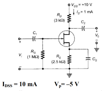
(Assume C1, C2 and Cs to be very large)

(Assume C1, C2 and Cs to be very large)
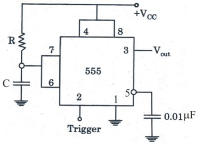
29. The circuit shown above is:

30. If the bias current in the IC-741 op-amp is IQ = 19 µA and the internal frequency compensation capacitor C1 = 30 pF, the slew rate of the op-amp will be nearly
Read More Section(Analog Electronics)
Each Section contains maximum 100 MCQs question on Analog Electronics. To get more questions visit other sections.
