41. For the junction transistor, which of the following relation is true?
42. An op-amp having input voltage Vi1 = 150 µV and Vi2 = 140 µV, differential gain Ad = 4000 and CMRR = 105. The output voltage of op-amp will be
43. The load impedance ZL of common emitter amplifier has R and L in series. The phase difference between output and input will be
44. Match List-I with List-II and select the correct answer using the options given below the lists:
List-I (Name of the circuit)
List-II (Characteristics of the circuit)
a. Darlington Amplifier
1. A circuit using pnp and npn transistors used in power amplifier.
b. Common base Amplifier
2. A Common-source Amplifier driving a common gate amplifier.
c. Complementary Symmetry Amplifier
3. A Circuit with overall voltage gain close to 1 and very large input impedance.
d. Cascode Amplifier
4. A Circuit with low input impedance mainly used in high frequency applications.
| List-I (Name of the circuit) | List-II (Characteristics of the circuit) |
| a. Darlington Amplifier | 1. A circuit using pnp and npn transistors used in power amplifier. |
| b. Common base Amplifier | 2. A Common-source Amplifier driving a common gate amplifier. |
| c. Complementary Symmetry Amplifier | 3. A Circuit with overall voltage gain close to 1 and very large input impedance. |
| d. Cascode Amplifier | 4. A Circuit with low input impedance mainly used in high frequency applications. |
45. The overall bandwidth of two identical voltage amplifiers connected in cascade will be:
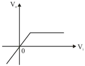
46. The voltage transfer characteristics as shown in the figure will relate to a
1. Voltage regulator
2. Half-wave rectifier
3. Full-wave rectifier
Which of the above is/are correct?

1. Voltage regulator
2. Half-wave rectifier
3. Full-wave rectifier
Which of the above is/are correct?

47. A 5 mV, 1 kHz sinusoidal signal is applied to the input of an op-amp integrator for which R = 100 kΩ and C = 1 µF. the output voltage is:
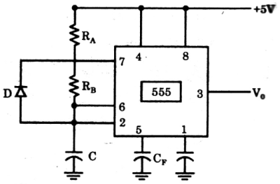
48. The function of the diode D in the timer circuit shown below is to


49. An op-amp is used as a zero-crossing detector. If the maximum output voltage is ±15 Volt p-p and the slew rate is 10 V/µsec, then the maximum frequency will be
50. A voltage VG is applied across a MOS capacitor with metal gate and p-type silicon substrate at T = 300 K. The inversion carrier density (in number of carriers per unit area) for VG = 0.8 V is 2 × 1011 cm-2. For VG = 1.3 V, the inversion carrier density is 4 × 1011 cm-2. What is the value of the inversion carrier density for VG = 1.8 V?
Read More Section(Analog Electronics)
Each Section contains maximum 100 MCQs question on Analog Electronics. To get more questions visit other sections.
