51. In a 3-input CMOS NAND gate, the substrate terminals of NMOS transistors are grounded (lowest potential available in the circuit) and the substrate terminals of PMOS transistors are connected to VDD (maximum positive potential in the circuit). Which of the following transistors may suffer in this circuit from body bias effect?
52. A 2-bit synchronous counter using two J-K flip flops is shown. The expressions for the inputs to the J-K flip flops are also shown in the figure. The output sequence of the counter starting from Q1Q2 = 00 is


53. Consider the following statements describing the property of a complementary MOS (CMOS) inverter:
1. It is a combination of an n-channel FET and a p-channel FET.
2. There is power dissipation when the input carriers the logical 1 signal.
3. There is no power dissipation when the input carries the logic 1 signal.
4. There is power dissipation during transition from 0 to 1 or from 1 to 0.
Which of the statements given above are correct:
54. For the Boolean expression $$\overline {\text{A}} {\text{BC}} + {\text{A}}\overline {\text{B}} {\text{C}} + {\text{AB}}\overline {\text{C}} {\text{,}}$$ how many 1's are in the output column of the truth table
55. The Boolean expression for the output of the logic circuit shown in the figure is


56. With the availability of 16 × 4 memory size, how many ICs (memory chips) will be required for the expansion of its word size in order to obtain 16 × 8 memory?
57. An X-Y flip-flop, whose characteristic table is given below is to be implemented using J-K flip-flop. This can be done making
X
Y
Qn+1
0
0
1
0
1
Qn
1
0
$${\overline {\text{Q}} _{\text{n}}}$$
1
1
0
| X | Y | Qn+1 |
| 0 | 0 | 1 |
| 0 | 1 | Qn |
| 1 | 0 | $${\overline {\text{Q}} _{\text{n}}}$$ |
| 1 | 1 | 0 |
58. The IC used for making a bidirectional universal shift register is-
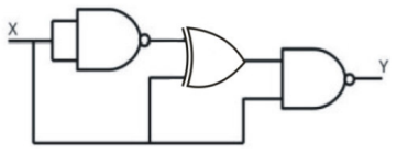
59. The output Y of the circuit shown below is


60. Consider the bit pattern 01010001. Which of the following has Hamming distance of exactly 2 from these patterns?
Read More Section(Digital Electronics)
Each Section contains maximum 100 MCQs question on Digital Electronics. To get more questions visit other sections.
