
ExamVeda
Login
Home
31
A monolithic metal oxide semiconductor (MOS) non-polarized capacitor which is a parallel plate capacitor with SiO2 as dielectric. A surface thin film of metal (aluminum) is the top plate. The bottom plate consists of the heavily doped n* region that is formed during emitter diffusion. What is the typical value of capacitance for an oxide thickness of 500 Å of this MOS capacitor?
Take the permittivity of dielectric (εr) as 4.
Discuss
Answer & Solution
Answer: Option D
No explanation is given for this question. Let's Discuss on Board
32
Which of the following holds FALSE for BJTs?
Discuss
Answer & Solution
Answer: Option B
No explanation is given for this question. Let's Discuss on Board
33
In order to ensure that the output voltage of an op-amp is zero, when both its inputs are grounded
Discuss
Answer & Solution
Answer: Option B
No explanation is given for this question. Let's Discuss on Board
34
If α = 0.98, ICO = 6 µA and IB = 100 µA for a transistor, then the value of IC will be
Discuss
Answer & Solution
Answer: Option D
No explanation is given for this question. Let's Discuss on Board
35
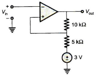
The circuit of figure uses an ideal Op-Amp for small positive values of Vin, the circuit works as
Analog Electronics mcq question image
Discuss
Answer & Solution
Answer: Option C
No explanation is given for this question. Let's Discuss on Board
36
For a common emitter. BJT configuration with collector terminal resistance R, the slope of the D.C. load line can be given by:
Discuss
Answer & Solution
Answer: Option D
No explanation is given for this question. Let's Discuss on Board
37
The value of hFE (the hybrid parameters) of a Common-Emitter (CE) connection of a Bipolar Junction Transistor (BJT) is given as 250. What is the value of αdc (ratio of collector current to emitter current), for this BJT?
Discuss
Answer & Solution
Answer: Option D
No explanation is given for this question. Let's Discuss on Board
38
Consider the following statements regarding an op-amp:
1. All types of negative feedback reduce nonlinear distortion.
2. All types of negative feedback reduce the output offset voltage.
3. Non-inverting (current and voltage) feedback increases the input impedance.
4. Inverting (current and voltage) feedback decreases input impedance.
Which of the above statements is/are correct?
Discuss
Answer & Solution
Answer: Option D
No explanation is given for this question. Let's Discuss on Board
39
For the operational amplifier circuit shown, the output saturation voltages are ±15 V. The upper and lower threshold voltages for the circuit are, respectively,
Analog Electronics mcq question image
Discuss
Answer & Solution
Answer: Option B
No explanation is given for this question. Let's Discuss on Board
40
In the given block diagram, which is the sampling element?
Analog Electronics mcq question image
Discuss
Answer & Solution
Answer: Option A
No explanation is given for this question. Let's Discuss on Board