
ExamVeda
Login
Home
11
Consider the circuit shown below. Find the output voltage V0 for input voltage Vi = 5 V. Assume the voltage drop across a conducting diode is 0.7 V.
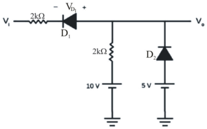
Analog Electronics mcq question image
Discuss
Answer & Solution
Answer: Option C
No explanation is given for this question. Let's Discuss on Board
12
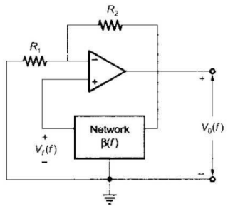
The circuit in the figure employs positive feedback and is intended to generate sinusoidal oscillation.
If at a frequency $${{\text{f}}_0},{\text{B}}\left( {\text{f}} \right) = \frac{{{{\text{V}}_{\text{f}}}\left( {\text{f}} \right)}}{{{{\text{V}}_0}\left( {\text{f}} \right)}} = \frac{1}{6}\angle {0^ \circ }$$     then to sustain oscillation at this frequency
Analog Electronics mcq question image
Discuss
Answer & Solution
Answer: Option A
No explanation is given for this question. Let's Discuss on Board
13
A bleeder resistor is used in a D.C power supply because it
Discuss
Answer & Solution
Answer: Option D
No explanation is given for this question. Let's Discuss on Board
14
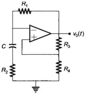
In the following astable multivibrator circuit, which properties of V0 (t) depend on R2?
Analog Electronics mcq question image
Discuss
Answer & Solution
Answer: Option A
No explanation is given for this question. Let's Discuss on Board
15
In a half-wave rectifier, if an a.c. supply is 60 Hz, then what is the a.c. ripple at output?
Discuss
Answer & Solution
Answer: Option B
No explanation is given for this question. Let's Discuss on Board
16
Consider an ideal long channel nMOSFET (enhancement-mode) with gate length 10 µm and width 100 µm. The product of electron mobility (µn) and oxide capacitance per unit are (Cox) is µnCox = 1 mA/V2. The threshold voltage of the transistor is 1 V. For a gate-to-source voltage VGS = [2 - sin(2t)] V and drain-to-source voltage VDS = 1 V (substrate connected to the source), the maximum value of the drain-to-source current is . . . . . . . .
Discuss
Answer & Solution
Answer: Option C
No explanation is given for this question. Let's Discuss on Board
17
An n-channel depletion MOSFET has following two points on its ID - VGS curve:
(i) VGS = 0 at ID = 12 mA and
(ii) VGS = -6 volts at Z0 = ∞
Which of the following Q-points will give the highest transconductance gain for small signals?
Discuss
Answer & Solution
Answer: Option D
No explanation is given for this question. Let's Discuss on Board
18
A full wave rectifier with a centre tapped transformer supplies dc current of 100 mA to a load resistance of 20Ω. The secondary resistance of transformer is 1Ω. Each diode has a forward resistance of 0.5Ω. What are rms values of signal voltage across each half of the secondary as well as dc power supplied to the load?
Discuss
Answer & Solution
Answer: Option A
No explanation is given for this question. Let's Discuss on Board
19
Two transistors have the same value of α but different gain bandwidth products. One of them is a germanium transistor and the other is a silicon transistor. Both the transistors have similar geometries and base width. The transistor with lower GB product.
Discuss
Answer & Solution
Answer: Option B
No explanation is given for this question. Let's Discuss on Board
20
A transistor RC coupled amplifier is designed for a voltage and band gain of 20. But a measurement at a particular frequency shows the gain to be only 14. What is the likely phase shift at this frequency?
Discuss
Answer & Solution
Answer: Option B
No explanation is given for this question. Let's Discuss on Board